Forum sponsored by:

Micro Slice Machine
| MW | 09/11/2016 13:50:18 |
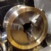 2052 forum posts 56 photos | Hi, So i've been looking at this machine, the microslice i'm sure what it does is nothing novel but what is promising is the relatively cheap construction of it for "lazering" pcb boards. I do quite like what it is trying to achieve. I'm puzzled by this though;
It's a sheet of copper thats been coated with spray acrylic black paint on both sides, lazered in the tracks a few times on a "relatively weak" 100mw lazer (by the creators own admission, although he promises a more powerful 250mw variant is in the works). It is then bathed in ferric cloride and cleaned up to give you this. So the hitch for me is why the lazer works on this, I thought PCBs needed etching into a special board where the copper is selectively etched away to isolate the electrically conductive copper from the boards special insulative coating, creating clear pathways for the current to flow. Here he has only sprayed a sheet of copper with acrylic and burnt away a few layers, is this really enough to isolate the current on the tracks from the rest of the copper sheet? Michael W Edited By Michael Walters on 09/11/2016 13:54:13 (typos) Edited By Michael Walters on 09/11/2016 13:56:18 |
| pgk pgk | 09/11/2016 13:58:50 |
| 2661 forum posts 294 photos |
From the loink you supplied: The tracks have to be engraved several times to make sure the laser cuts through both the paint and any residue left behind. After the laser has done its work the PCB is put into a Ferric Chloride bath and agitated for about an hour. By holding the cleaned PCB up to a light you can check the etching has cut all the way through the exposed copper. If it hasn't quite worked it can be put back in the etching solution for a bit longer. & While it is possible to make PCBs using the MicroSlice the process isn't perfect. So far I have only been able to etch the PCB effectively by using the new 250mw diode unlocked at the £55,00 Stretch Goal. I have not been able to do it successfully using the 100mw diode. Hopefully this won't be a problem as the £65,000 Stretch Goal which unlocks a 200mw diode for the Standard kit isn't too far away!
|
| Tomfilery | 09/11/2016 15:18:21 |
| 144 forum posts 4 photos | Michael, I presume that he has missed out some words and that what he actually meant was that he painted a piece of copper-clad printed circuit board material and therefore, all he was doing was burning the paint off with the laser, so that the ferric chloride could get at the copperand etch it away. PCB material is an insulator with a thin layer of copper attached to one or both sides. There a quite a few people doing their pre-etch "marking out" that way with many references to it on the web. Regards Tom |
| MW | 09/11/2016 15:36:37 |
2052 forum posts 56 photos | Posted by Tomfilery on 09/11/2016 15:18:21:
Michael, I presume that he has missed out some words and that what he actually meant was that he painted a piece of copper-clad printed circuit board material and therefore, all he was doing was burning the paint off with the laser, so that the ferric chloride could get at the copperand etch it away. PCB material is an insulator with a thin layer of copper attached to one or both sides. There a quite a few people doing their pre-etch "marking out" that way with many references to it on the web. Regards Tom Ah, that would explain why there is a circuit in the first place! I didn't realize that it's no ordinary copper sheet, you can't see the side of it on the image so it just looks like plain copper, thank you. I think the black paint is to help the lazer cut into it because they don't like bright colours, it would hardly touch the reflective copper so it's there to help absorb the light rays. Michael W Edited By Michael Walters on 09/11/2016 15:38:09 |
| Tomfilery | 09/11/2016 15:56:40 |
| 144 forum posts 4 photos | Michael, Sorry, but you still have it wrong, I'm afraid. As you correctly say, the laser will not touch the copper. All he is doing is using the laser to burn away the paint, so that the ferric chloride can get at the thin copper film on the insulator and etch it away. So, everywhere the laser has burned away the paint, the copper will be exposed. Where there is only untouched paint, the ferric chloride cannot etch and the copper will remain intact. Hope this is now clear. Regards Tom |
| MW | 09/11/2016 16:00:57 |
2052 forum posts 56 photos | Yes thank you tom, thank you for the explanation. Michael W |

Please login to post a reply.
Magazine Locator
Want the latest issue of Model Engineer or Model Engineers' Workshop? Use our magazine locator links to find your nearest stockist!
Sign up to our Newsletter
Sign up to our newsletter and get a free digital issue.
You can unsubscribe at anytime. View our privacy policy at www.mortons.co.uk/privacy
Latest Forum Posts
- *Oct 2023: FORUM MIGRATION TIMELINE*
05/10/2023 07:57:11 - Making ER11 collet chuck
05/10/2023 07:56:24 - What did you do today? 2023
05/10/2023 07:25:01 - Orrery
05/10/2023 06:00:41 - Wera hand-tools
05/10/2023 05:47:07 - New member
05/10/2023 04:40:11 - Problems with external pot on at1 vfd
05/10/2023 00:06:32 - Drain plug
04/10/2023 23:36:17 - digi phase converter for 10 machines.....
04/10/2023 23:13:48 - Winter Storage Of Locomotives
04/10/2023 21:02:11 - More Latest Posts...
- View All Topics
Support Our Partners


Shopping Partners
Subscription Offer

Latest "For Sale" Ads
- Reeves** - Rebuilt Royal Scot by Martin Evans
by John Broughton
£300.00 - BRITANNIA 5" GAUGE James Perrier
by Jon Seabright 1
£2,500.00 - Drill Grinder - for restoration
by Nigel Graham 2
£0.00 - WARCO WM18 MILLING MACHINE
by Alex Chudley
£1,200.00 - MYFORD SUPER 7 LATHE
by Alex Chudley
£2,000.00 - More "For Sale" Ads...
Latest "Wanted" Ads
- D1-3 backplate
by Michael Horley
Price Not Specified - fixed steady for a Colchester bantam mark1 800
by George Jervis
Price Not Specified - lbsc pansy
by JACK SIDEBOTHAM
Price Not Specified - Pratt Burnerd multifit chuck key.
by Tim Riome
Price Not Specified - BANDSAW BLADE WELDER
by HUGH
Price Not Specified - More "Wanted" Ads...
Get In Touch!
Do you want to contact the Model Engineer and Model Engineers' Workshop team?
You can contact us by phone, mail or email about the magazines including becoming a contributor, submitting reader's letters or making queries about articles. You can also get in touch about this website, advertising or other general issues.
Click THIS LINK for full contact details.
For subscription issues please see THIS LINK.
Digital Back Issues


Donate

 Register
 Log-in
Model Engineer Magazine
- Percival Marshall
- M.E. History
- LittleLEC
- M.E. Clock

ME Workshop
- An Adcock
- & Shipley
- Horizontal
- Mill
Subscribe Now
- Great savings
- Delivered to your door

Pre-order your copy!
- Delivered to your doorstep!
- Free UK delivery!
All Forum Topics > CNC machines, Home builds, Conversions, ELS, automation, software, etc tools > Micro Slice Machine